We’re going to be at the Fort Wayne Maker Faire this weekend. If you’re in the area come by and say hi!
We’re going to be at the Fort Wayne Maker Faire this weekend. If you’re in the area come by and say hi!
Our booth at the Detroit Maker Faire. We had a great time meeting people and showing off our stuff. There were a lot more people than the pictures might suggest, but I was busy talking to those people and only had a chance to snap pics during the lulls 🙂
Next, we’ll be at the Fort Wayne Maker Faire in a couple weeks.


We’ve been working on bringing our hypno-effects to string lights for some time now, and just launched a Kickstarter campaign to help fund our first production order! Check it out here: hypnocube.com/kickstarter


On several recent microcontroller projects I have needed to store settings in microcontroller flash, and since flash erase/write cycles are fairly limited, I had to pack bits carefully to ensure that gadget lifetimes would be usable. To increase flash lifetime, error correction codes are often used to mitigate flash failures, but different error correction codes work best for certain error patterns, so I wanted to test how bits fails in flash. Knowing details about bit failure modes, patterns, and related issues would help select an error correcting code that is most useful for my combination of needs and restrictions. I could not find the information I wanted, so I decided to test my devices. This article details the flash bit failures for the device I tested, and hopefully is useful for similar devices and designers.
To gather the relevant data, I wrote code that repeatedly erased/wrote flash memory, logging all bit failures so I could analyze them. Over a period of about a day and a half I gathered about 1 million erase/write cycles from microcontroller flash, logged over 40 million bit failures, learned quite a bit about flash memory in the process. The results are interesting and are the reason for this article.
Here is a screenshot showing the bit errors after the million erase/write cycle run. Details are below, and a video of it is at https://www.youtube.com/watch?v=7elfyRyW5ms.

Since flash degrades over time from erasing/writing (or even just reading, although that decay is slower), if the decay modes are understood, then error correction codes can be designed to improve the length of time before a system fails. However the two main error codes recommended, Reed Solomon and BCH codes, are suited for different failure patterns. Without getting into the details (that may be another article), Reed Solomon is more useful for bit errors that occur bursts, which BCH codes are better for bit errors that are uniformly distributed. (Informally, both work over finite fields of size 2^n, and RS codes correct field elements, i.e., n bits at a time, while BCH codes correct at the single bit level).
Another issue was the devices I was using listed erase/cycle lifetime of about 20,000 cycles, and I wanted to test some devices to see how accurate this is. Turns out the flash is likely useful for many, many more cycles than the spec sheet (conservatively) lists.
To help explain the results, it is useful to cover the physical level of flash storage. I will do it in two levels of detail, basic and advanced.
At the physical level, flash memory stores logical 0 and 1 as electrons trapped inside insulated cells. The electric field inside these cells are read by transistors that use the field strength to detect if the charge in the cell passes some threshold or not. Erasing flash is done by pulling the electrons out of the relevant cells using large voltage potentials, and writing is done by putting electrons in the cells, often through “hot electron” injection which is done by creating highly energetic electrons that can pass the insulating barrier. Over time these cells degrade through a combination of electrons getting trapped in the insulating materials, which makes the threshold hard to identify, and through physical damage to the cell from repeated hot electron injection. As the insulator breaks down, the charge no longer remains trapped. The end result is flash memory cells degrade over time.
If you’re comfortable with this level of physical representation of flash, skip ahead to the experiment. If you want a lot more physical details, read the next section on advanced flash memory operation.
Since I wanted this to be approachable to non-physicists/non-solid state people, I’ll explain how flash memory works starting at a very low level: atoms and electrons. I’ll try to cover briefly and mostly qualitatively how flash memory works from fundamental physics on up.
The net result of this section is materials can be created that have an excess or lack of electrons, which in turn affects how easily it is to get electrons to move through such materials, and that placing different materials next to each other can cause useful electron effects at the resulting boundaries.
Electron behavior is most accurately treated by quantum field theories (QFTs, the Standard Model in particular), which are a bit too abstract for this article, so I will treat electrons (incorrectly, but illustratively) as little balls with charge that orbit the nucleus of an atom, adding the non-classical behavior of being able to quantum tunnel through energy barriers. Electrons have a -1 charge, and each proton in the nucleus has a +1 charge. As described theoretically by QFTs (or less precisely by quantum mechanics), and as determined experimentally, electrons bound in atom orbits have discrete energy levels. Also as described theoretically and determined experimentally, opposite charges attract and like charges repel. These basic physics facts drive most of how solid state devices work (to get an accurate quantitative model takes a lot more quantum mechanics and solid state physics, but this simple level gives a good understanding).
Electrons on a single atom are allowed to take discrete energy levels, and through the requirements from spherical harmonics, these energy levels can be computed and described quite accurately. Spherical harmonics are simply the math giving solutions to which periodic waves have spherical symmetry. From this math the electrons form energy “shells” and “subshells,” which are just useful ways to classify the different electron energy levels. The outermost shell (with some exceptions) interacts with other atoms to form larger structures.

(The most common isotope of) silicon, for example, has 14 protons, 14 electrons, and 14 neutrons. The electrons are arranged in three shells containing 2, 8, and 4 electrons in increasing energy levels, with the nomenclature 1s^2 2s^2 2p^6 3s^2 3p^2. The initial number in each term denotes the shell, the ‘s’ and ‘p’ denote subshells (names are from historical messiness), and the powers denote the number of electrons in each subshell. That the outer shell has exactly 4 electrons is very important for semiconductors. Ignore the ‘k’,’l’,’m’ in the diagram.
Atoms bond with each other to form larger structures by trying to form lower energy states, which includes trying to fill electron shells and/or taking electrons from atoms that have weaker hold on them (with the resulting + and – charged ions then forming ionic bonds). A common bond type in semiconductors is the covalent bond: neighboring atoms share electrons to try and fill their outer shells with 8 electrons.
As atoms form solids, electrons interact and “smear” across larger regions, causing the allowed energy levels to “split” into refinements. The net result is there are still discrete energy levels, but they tend to come in bunches, forming what are called “bands” and “gaps” in solid state physics. Bands are where there is a dense collection of energy levels, and gaps are an energy range where there are no allowed electron states.
When the system is at the lowest energy state (absolute zero temperature, for example), the electrons tend to stay in the outer shell, called the valence shell. The resulting energy levels are the valence band. As temperature increases, or voltage (explained below) is applied, more and more electrons leave the valence band for higher energy states, called the conduction band, and this movement allows electric current to flow.
Just like a gravity field is a force that attracts mass, an electric field is a force that attracts (or repels) electric charge. The strength of a gravitational field is similar to voltage: a stronger gravitational field causes masses to accelerate more, and a higher voltage causes an electric charge to accelerate more. This is needed to understand how electrons are moved about in semiconductors, and in particular, flash memory.
The higher view of electricity using volts, amps, and ohms, can all be modeled using how electrons move in solids. Current is the flow of electrons, with an amp denoting the movement of one coulomb of charge per second past some point. A coulomb is a quantity of charge containing 6.241×10^18 electrons. Voltage measures the potential difference between two points, and gives the force that pulls at each electron. One volt can be defined as the potential difference between two infinite parallel conducting plates 1 meter apart that creates a force of 1 Newton per coulomb. Double the volts, and I doubles the force. For scale, 1 Newton is roughly the force of gravity at Earth’s surface on 102 grams.
Intuitively, voltage is how much force is pulling on electrons, making them move, and current is how many move per unit time.

Different materials allow electrons to move more or less easily, and the ease of movement is called conductivity. Conductivity is defined as the current (in amps per square meter) divided by the electric field strength (in volts per meter). The reciprocal is resistivity. Many factors influence conductivity, such as how many electrons are in outer shells of a material, how strongly they are held, temperature, etc.
In some materials, the outer (valence shell) electrons are tightly held in the atoms or molecular structure, and the high potential required to make them move results in electrical insulators. In other materials the valence electrons move much more easily, making conductors. This can all be computed from basic electron structures with enough magic.
The ease that materials allow electrons to move about in the presence of an electric field is called conductivity, and the reciprocal is called resistivity. At a given voltage (think gravitational pull for charges), a more conductive material will allow more electrons to flow, and the rate of electron flow (the flux) is called current. Increase the voltage, and the current will increase. All of this is somewhat simplistic, but accurate to first order, and illustrative of how devices work.
The image shows energy levels for a few types of materials.
Elements are organized in the periodic table into columns that give a first approximation to outer electron behavior. Those with 4 outer electrons (Group IV, including silicon, carbon, and germanium) contains what are called “elemental semiconductors,” which are materials with conductivity that lies somewhat between conductors and insulators. In general, a conductor has around 1 to 2 freely moving electrons per atom, semiconductors have 1 around freely moving electron per 10^7 to 10^17 atom.
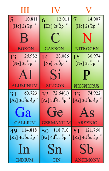
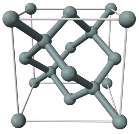
The outer shell for atoms in this (and most parts) of the periodic table try to grab 8 outer electrons (which is why the noble gases, with 8 outer electrons already, do not easily form compounds). Since each in Group IV comes with 4 already, they each want 4 more. Forming a crystal of carbon, silicon, or germanium causes the atoms to form a diamond cubic crystal lattice, in which each atom sits at the center of a tetrahedron, and connects to 4 neighbors. In this form, each atom has shares the 4 outer electrons with 4 neighbors, and each neighbor shares one back. Think of each atom as getting the desired 8 outer electrons part of the time, and sharing part of the time.
The lattice of silicon and some other group IV elements can be viewed as having atoms at each corner and face of a cube, with bonds shared as in the diagram. The electrons forming bonds pull the lattice together and the positive charges in the nucleus repel to hold the spacing apart.
As a simple example of a basic computation, look at one primitive cell of silicon (pictured). A good estimate of the side length of such a cube can be computed from knowing a few basic facts: the atomic weight of silicon is about 28, Avogadro’s number is 6.022×10^23, and the density is 2.3290 g/cm^3. Counting how many atoms exist in each primitive cell, each corner atom is shared by 8 cells, each face atom is shared by 2, so there are (8 corners/8 shared) + (6 faces/2 per face) + 4 interior = 1+3+4=8 atoms per primitive cell. Thus in 2.3290 grams of silicon there are 2.3290/(8*28/(6.022×10^23))= 6.26127*10^21 cells, which makes a cube with (6.26127*10^21)^(1/3)= 1.84312*10^7 cells per side, so each measures 1/1.84312*10^7 = 5.42558*10^-8 cm = 5.43 Angstroms per side.
Of these Group IV elements, silicon is used as the basis for modern semiconductors, because of multiple reasons: it forms high quality compounds like the insulator silicon dioxide (SiO2), it has a nice band gap (long story!) of 1.1 eV, making it perform well at room temperatures, it is cheap, and it is easy to build into low defect atomic structures.
Atoms from neighboring columns of the periodic table have either 3 or 5 outer shell electrons, and carefully mixing them in when making the silicon lattice results in a material with either more or fewer electrons than the eight per outer shell that pure silicon would give. These atoms take the place in the lattice of what would have otherwise been silicon.
Adding Group V phosphorus (P) adds one free electron per atom which can move much more freely than electrons in pure silicon, increasing conductivity. Adding Group III aluminum (Al) would result in one fewer electron per Al atom, and now instead of an excess electron, there is a shell missing an outer electron, which results in a pull on any electron to try and fill the shell.
Any resulting excess electrons move much more easily than the eight ones bound in cells, and any deficit of electrons results in ‘holes’, which are places an electron is pulled into the missing slot to fill an outer shell. In the theory of solids and semiconductors, these holes are treated as particles, since as electrons are pulled in, the ‘hole’ effectively moves around the lattice. So conceptually this hole is thought of as a moving positive charge, when in fact it is physically merely a pull on negative charges (electrons) to fill the hole.
Adding these electron rich or poor atoms to the silicon lattice is called doping, with the added elements called dopants. Boron, which has only three outer shell electrons, is the most widely used group III dopant, and resulting group III doped materials are called p-type materials, meaning they have excess positive charges (holes). Phosphorus and arsenic are the most widely used group IV dopants, and with 5 electrons in their outer shells, are called n-type dopants, since they have excess negative charges.
The result of careful adding of the right amount of the right kinds of atoms to the silicon crystal as it is formed can change the conductivity drastically. Substitution of just one dopant atom per 10^7 atoms of Si can increase the conductivity by a factor of 100,000.
Now I can explain how flash memory works.

Flash memory is made using individual physical “cells” to store logical values, with physical structure as in the diagram. The N and P materials are dopes silicon, and the insulator is usually silicon dioxide.
For current to flow from source to drain, it must pass through the n-type source, the p-type base, and then the n-type drain. At each n-type to p-type boundary, the holes in the p-type material attract electrons from the n-type, pulling them across, filling some of the holes. This creates a potential barrier, so a higher amount of voltage is required to get electrons to flow than if there was only one type of material.
Now, if the floating gate is has no net charge, and enough positive charge is applied to the control gate, then electrons are pulled from lower regions in the p-type material towards the control gate at the top, making more electrons available between the source and drain. This allows current to flow at a lower source to drain voltage, since there are more electrons in the conduction band along the top of the p-type material. Both the control and source to drain voltage are carefully measured.
If electrons are stored in the insulated floating gate, then the field from the positive charge on the control gate is somewhat hidden (or shielded, or cancelled out) by the electrons in the floating gate, and so fewer electrons get pulled into the into the conduction band in the p-type material below. The result is a higher voltage needs applied to the control gate to allow the same current to flow from the source to drain as before.
The lowest control gate voltage that allows a certain current to flow is measured, and the difference is used to differentiate between amounts of electrons in the floating gate.
In single level cells (SLC flash) the charge is treated as on or off. In multi-level cells (MLC) different amount of electrons are stored, representing multiple bits per cell, at the cost of being less robust, noisier, more prone to error, etc. For MLC the control gate voltage needs to be able to differentiate between more states in the floating gate.
In order to be erasable, writable, the floating gate needs to store electrons without applied power, thus needs to be insulated, and needs to have electrons added and removed to set the logical states.
The insulating layer is silicon dioxide, which has to a very precise thickness: lower thickness allows lower voltage operation, but also allows more leakage over time. It cannot be thinner than about 7nm if data retention of 10 years needed. Too thick and it’s slower and takes higher voltage to program the cell.
Programming is the act of placing electrons into the floating gate, and is often done by hot electron injection or sometimes by quantum tunneling (of a sub-type called Fowler-Nordheim tunneling).
In hot electron injection, a large enough voltage is formed from source to drain to cause electrons to accelerate from source to drain with enough energy to penetrate the insulating material. To get them to turn upwards and enter the floating gate, enough voltage is applied to the control gate to turn them. To get enough electrons into the floating gate in the programming time, the variations on voltages, materials, operating temperature, etc., all come into play. Lower current means less electrons generated and lower voltage means lower electron energy which both mean longer programming time. In general electron energy needs to be near 3eV, and it’s common to float the drain, place +6V on the control gate, and -5V on the source. These higher voltages are created on chip using voltage pumps.
In quantum tunneling, lower energy electrons are used, at the cost of slower programming time. A benefit is a decrease in physical damage over time to the materials. In practice both effects contribute.
Programming damages the insulator over time, electrons get trapped in the insulating material and nearby material, and the insulator is physical damage from being bombarded with high energy electrons, so over time breakdowns in the ability to add or remove or store electrons contribute to flash memory wearing out.
To erase the cell, the electrons need removed, and this is done almost exclusively by quantum tunneling, which is done by putting enough potential across the gate and base to allow the electrons in the insulated region to quantum tunnel out. Quantum tunneling is not like a classical tunnel being bored – it is more like a teleportation where the electron just “jumps” out. Quantum tunneling allows electrons to jump over energy barriers that a classical particle could not overcome, and the probability of how and where it jumps is related to the size of the energy barrier involved. By increasing the voltage across the gate and base, the energy barriers are effective lowered enough that the electrons have a large enough probability of jumping out that erasure occurs. However, when and where the electron jumps to is probabilistic, so there is some change it just jumps into the insulator. Similarly, excess electrons may tunnel out of the insulator, making the effect less damaging.
For SLC flash, when the memory is erased via quantum tunneling, the memory reports this as a logical ‘1’, and when the container holds enough electrons, the memory reports a logical ‘0’. This process is inherently slower than programming, which is why erasing flash is slower than writing. For MLC and TLC different electric field levels correspond to different bit patterns.
Finally, a final failure mode in flash is caused by electric charge in neighboring cells and nearby material causing the desired cell to read incorrectly due to those charges contributing to the electric field strength of nearby bits. As cells are made smaller and smaller, this becomes more of an issue.
Flash memory comes in two main types, NAND and NOR (named after some of the underlying gates), one difference being whether or not the memory allows random read accesses. NAND allows memory to be erased or written in blocks, while NOR allows single cells to be read. Since NOR requires more circuitry, it is more expensive per cell. As a result of NOR allowing individual cell access, most microcontrollers use NOR for storing execute-in-place code, since it is more efficient to execute code from memory allowing random access. NAND is cheaper, thus used for long term storage in many other devices like iPads and SSD drives.
NAND flash is accessed like block devices, each block consists of pages (sizes of 512, 2048, and 4096 are common). Reading and writing are page level, erasure is block level. To execute code form NAND, it is usually copied to RAM first, using some form of memory management unit. Additional bytes add error correction to increase reliability and lifetime, and many devices have sophisticated memory controllers that perform wear leveling to increase lifetime. Microcontrollers rarely have this level of support for the flash in them.
Both NAND and NOR erase a page at a time (or sometimes more).
Finally, Wikipedia lists common write endurance of
Here is the experiment we did on an actual device to see how flash degrades. The microcontroller we used is a PIC32MX150F128B [PIC150], mostly because we already had many nicely hackable boards we developed using this PIC in the form of our HypnoLSD modules (LED strand controllers, pictured). This PIC has 32K of RAM and we ran it at 48MHZ with a 1Mbaud serial connection to output logging data. We ran 1 million erase/write cycles on a device rated for 20,000 erase/write cycles.

This PIC has 128K of NOR flash and an additional 3K of flash for a boot loader. The flash page size is 1024 bytes, row size is 128 bytes, and the flash is addressable as 32-bit words. The hardware has support for
Even though the smallest possible writeable section of flash is a 32-bit word, before we undertook this experiment (and I learned details on how flash worked), I noticed erasing flash sets all bits to 1, and I could progressively write 0 bits to any location by properly reading a word, setting the proper bits, and writing the word back. This allowed storing the changes I needed in smaller portions of flash by incrementally setting fields.
For an idea of what this flash looks like on a die, [siliconporn] has a die shot of a related PIC device, the PIC32MX340F512H (512K flash, 32K RAM), which has a bit cell pitch of 1015×676 nm (which is 0.686 μm^2/bit); I suspect the PIC we tested is made with similar size gates. I could not find a die shot of our particular PIC.

Based on how bits fail from the above details on how flash works, I expected once a bit failed it would later work again, then fail again, etc. Thus I only wanted to log changes between failing and succeeding in order to lessen the amount of messages logged. To track these changes I needed RAM buffers to compare last state and new state for each bit tested in flash for both the last erased result and the last written result, requiring 2 bytes of RAM for each 1 byte of flash tested. Since some RAM was used for variables, I chose to use 4K of RAM for testing 2K of flash at a time, with 8 such regions testable, selectable while running.
This allowed testing two flash pages (256 words = 1024 bytes each) at a time.
The code on the PIC is a small C application that sets up the hardware, then loops over erase/write cycles, writing any failures to the output serial port. I logged the output to a file, which took around 34 hours to log 1,000,000 erase/write cycles. Later cycles got much slower as more errors were reported. If I run this again, I’ll set the logging speed to 3 or even 12 Mbps to speed up the overall process. The code for the PIC portion is at https://github.com/ChrisAtHypnocube/FlashWrecker.
In slightly more detail, the code loops over the following:
The resulting log file is 4.6GB of text which has the form:
...
Pass 723466, frame 0, offset 00000000, time 908b5feb, errors 824483
ERROR: (E) offset 0000001E read FFFFFFFB desired FFFFFF7B.
ERROR: (E) offset 00000046 read FFFFFFFF desired 7FFFFFFF.
ERROR: (E) offset 00000084 read EFFFFFFF desired FFFFFFFF.
ERROR: (E) offset 0000008E read FFEFFFFF desired FFFFFFFF.
ERROR: (E) offset 000000B7 read FFFFFFDF desired FFFFFFFF.
ERROR: (E) offset 000000C4 read FFFBFFFF desired FFFFFFFF.
ERROR: (E) offset 000001B8 read FF7FFFFF desired 7F7FFFFF.
ERROR: (E) offset 000001BE read 7FFFFFFF desired FFFFFFFF.
ERROR: (E) offset 000001D2 read FFFFFF7F desired FFFFFFFF.
Pass 723467, frame 0, offset 00000000, time 90aea31f, errors 824492
ERROR: (E) offset 00000046 read 7FFFFFFF desired FFFFFFFF.
...
The logs contain an erase/write pass number, the memory offset into my reserved flash region (frame is 0-7 to select different parts of the region to test), a time in the form of an internal 32-bit CPU core tick, and the number of errors so far detected (technically, these are both errors and later corrections when that failed bit works again, so it is roughly a double count of bit failures).
For each pass, each word is checked against what it should be, as recorded by what it was last time the state was attempted on that flash word. A memory offset is output, what was read at that location, and what was recorded in RAM as the last read value from that location. Then the RAM is updated, and the cycle continues. The error type (E) or (W) denotes an error in the erase or write phase.
Logging was done by adding file logging support for our Hypnocube device controller (https://github.com/ChrisAtHypnocube/HypnoController), which allowed me to quickly develop a method to run the experiment. Any decent logging serial terminal would do as well, but I wanted to make sure it supported huge files, used different threads for reading and writing to avoid missing any inputs at high speeds, and flushed messages to the file properly in case of something crashing. Writing my own logging based on our existing code ensured these goals were met.
After a few initial passes on a first device to get all related software parts working, we programmed a new PIC and started recording output. One and a half days later we reached 1.1 million passes, with over 40 million bit errors, and decided to stop and analyze the data.
To analyze the data, I made a second C#/WPF program (at https://github.com/ChrisAtHypnocube/FlashWreckAnalyzer) that reads in the log file, allows interactive visualization of the time changes of the flash, computes some stats, and ultimately creates a visualization of the flash degradation.
The main thing I wanted to test is the accuracy of the statement: “each bit is independently likely to fail, with exponential dependence on number of erase/write cycles”.
A final visualization of the million frame degradation is at https://www.youtube.com/watch?v=7elfyRyW5ms . Here is the final frame of the visualization:
In the picture (and animation) bits are laid out 32 to a word, 4 words to a row, and 64 rows to a flash page. The erase/write cycle just ended is listed in large letters.
On the right are two bars that move up during the animation: the left blue one is the frame, and the right one stays at the same height showing an error graph, with width from 0 to the max number of errors detected.
White/gray bits have not failed, light red bits have failed on an erase and remain failed, light blue bits have failed previously but erased on the last attempt, and the richer/bigger red and blue bits have done the same but exactly on this cycle. We had no write failures, so I did not put colors for them in the legend, but they are in the code.
Below are some other stats, like elapsed time, and some other stats, explained below.
First failed bit happened on cycle 229,038 at bit index 8207. A separate run on a separate device had a first bit failure around cycle 400,000. So (given the small sample size of 2!) it appears that 20,000 cycles is quite conservative. I could not find a detailed description of how Microchip arrived at their value; perhaps it was an earlier manufacturing process, and the data sheets are out of date.
The first thing we noticed from the image above is that the failed bits seem to prefer certain horizontal regions. To look for other patterns, I gathered lots of stats on the failed bit patterns.
Some are shown on the screen; here are descriptions and comments. For each value of N in 0, 1, …, 31, I recorded
Besides these stats shown on the visualization, other stats were computed and saved at the end. Here are graphs and commentary. Each is described as y-axis value versus x-axis value.
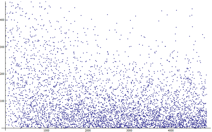
#2 from above should be nearly a straight line; instead we get this plot of number of bit errors versus bit index in a word of 0, 1, …, 31. A distribution this skewed is very unlikely.
Plot of cycle where a new bit failed versus bit failed count (4857 total failed bits). This graph is what I would expect.

Gaps between successive new bit failures versus bit failure count. Again, nicely spread.
Bit position 0-16385 versus order the bits failed. Here you start to notice banding in 4 strips….

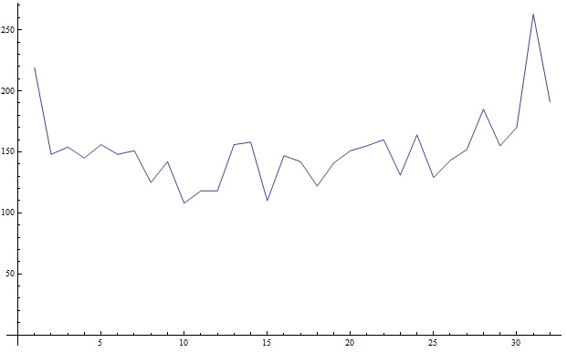
The above (and the visualization) lead to inspecting the number of failures per row (a row in the PIC is 128 bytes). The number of failures per row is 428,432,170,157,477,474,151,166,390,384,172,183,480,471,163,159. This is a graph of failures per row versus row 0-15:

This clearly looks like some underlying factor is biasing the failures. A quick estimate to check how likely this could happen randomly gives: there were 4857 failed bits out of 16384 monitored, if we assume bits are equally to fail, we can ask the question: what is the probability eight rows have a total at most 183, and eight rows have a total at least 384. The probability of this happening if bits are uniformly likely to fail is less than one in 10^-134, so not likely. This is a clear bias.
Once a bit failed, it usually started working again, then failed again, then worked again, etc… I would expect that the lengths of the working state would decrease, and the lengths of the failed state would increase. To check this for one bit, I took the first bit to fail (since it recorded a lot of success/fail transitions), and computed all the lengths of each mode. There were 7293 intervals where the bit as failing, and 7293 regions where the bit was working (after the first fail). The result is very noisy, making it hard to visualize. However, taking moving averages over 1000 samples at a time results in the following:
Moving average length of intervals where first bit is working versus sample index (moving average over 1000 samples):

As expected, the success interval length decreases over time, but is not very smoothly doing so.
Doing the same for the failed interval lengths: moving average length of intervals where first bit is failing versus sample index (moving average over 1000 samples):

This somewhat increased, but again is very messy. I’m not sure how to interpret these two graphs nor what to do to refine my knowledge.
A similar stat is gathering all runs from all bits, and counting how many times each length occurs, and plotting them.
Lengths of successful run intervals, showing the first 80K out of 107097 entries, using a moving average of 1000 entries, versus length

Lengths of failed run intervals, showing the first 80K out of 107097 entries, using a moving average of 1000 entries, versus length

These show that long runs where a bit has failed are not as likely as short runs, with the decrease fairly well behaved. The runs for the successful are not as well behaved, but they too decrease with length.
A final interesting point is we noticed no failures to write a bit, only failures to erase a bit.
Conclusions, things to do in the future, and other final points
8) It would be interesting to search the data for other types of bias, and to get a good die shot of the PIC, and figure out what causes the biases we found.
Finally, since the errors in this flash are pretty well spread over random bits, and not in bursts (except for the row bias), BCH codes are a better choice for error correction in these devices.
[HypnoLSD] http://hypnocube.com/products/controllers/hypnolsd/
[siliconporn] http://siliconpr0n.org/archive/doku.php?id=azonenberg:microchip:pic32mx340f512h
[video1] https://www.youtube.com/watch?v=7elfyRyW5ms
[PIC150] http://www.microchip.com/wwwproducts/Devices.aspx?product=PIC32MX150F128B
The World Maker Faire in New York City is this weekend and we’ll be there for the second year! We’re (almost certainly) going to be in the Viscusi Gallery, upstairs inside the New York Hall of Science building. Come say hi and check out what we’re working on!
![]()
